We are a leading manufacturer of quality internal and external lighting products for commercial, industrial and retail applications.
View all productsAt Ansell Lighting we design and manufacture an extensive range of luminaires for a diverse number of sectors and applications. Whatever the shape, purpose or style of your space, we have a lighting solution.
View all sectors & applicationsWe are a leading manufacturer of quality internal and external lighting products for commercial, industrial and retail applications.
Welcome to Ansell lightingWe are here to answer any questions you may have, help you find a stockist or speak to a local member of our team.
OCTO delivers the complete smart lighting package to transform the efficiency and ambience of commercial and residential spaces.
Find information regarding our product warranty, product data downloads and FAQs regarding lighting and technical terms. Here you will find support with training CPDs as well as useful lighting design and LED strip calculators.
Physics of LED

An LED is more properly known as “Light Emitting Diode” and, as the name suggests, normally consist of a single p-n junction diode, which is the basic building block of solid-state electronics and is the simplest possible semi-conductor device, where the fundamental electrical property of a semi-conductor diode is that it only allows electric current to flow in one direction.
The LED is the type of semiconductor which combines a P-type semiconductor with an N-type semiconductor, where the P-type layer has a deficit of electrons, or a surfeit concentration of holes, thereby making it positively charged, whereas the N-type layer has a large concentration of negatively charged particles thereby making it negatively charged.
Due to the electrostatic attraction between positive and negative particles, the free electrons are attracted towards the positively charged holes, as shown in the image below, and the diode is a very simple device which uses one piece of N-type material, having an excess of electrons, connected to another piece of P-type material having an excess of holes, with the area at the point where the two materials meet being known as the “Junction Point”.
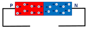
Initially the N-type material on the right has too many electrons and the P-type material on the left has too few electrons, which causes an imbalance in the circuit, and where the electrons and holes will tend to move towards each other attracted by their opposing electrostatic charges. Where a hole and electron meet, they will cancel each other out forming a neutral area of paired holes and electrons and this situation will continue until the formation of a “depletion zone” on either side of the junction point where everything is nicely balanced out and all the surplus holes and electrons are used up, as shown in the image below.
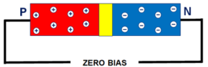
In the depletion zone, the semi-conductor is essentially restored to its original, pre-doping state where there are no free electrons to carry current, so it behaves, once again, as an insulator. In this state, and without externally applied voltage, the diode remains an insulator which would not allow any current to pass. To get current flowing through the device you have to encourage the free electrons on the right in the N-type material to move towards the P-type material on the left and vice-versa, thereby attempting to overcome the yellow depletion zone.
By connecting the P-type material to the positive terminal of a power source and the N-type material to the negative terminal of the same power source, as shown in the image below, an electric field can then be created across the diode, however before the P-N junction can be used as a practical device, there is a need to ‘bias’ the junction, which is basically the connection of a voltage potential across it.
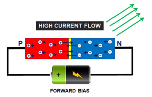
When the diode is connected in a ‘Forward Bias’ condition, a positive voltage is applied to the P-type material and a negative voltage is applied to the N-type material, as shown in the image below. When the external voltage becomes greater than the value of the barrier, the potential opposition will be overcome, meaning that an electric field can then be created across the diode, and the resulting current will start to flow. This is because the free electrons will be attracted towards the positive electrode and repelled from the negative one, and similarly, the holes will be attracted towards the negative electrode and repelled by the positive ones.
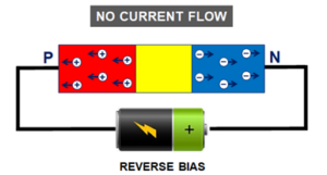
When the diode is connected in what is known as a ‘Reverse Bias’ condition, as shown in the image below, the positive terminal voltage is applied to the N-type material and the negative terminal voltage is applied to the P-type material. The opposite then happens, in that the electrons retreat even further towards the positive electrode and the holes towards the negative resulting in a much wider depletion zone and in this state, the diode becomes an even greater insulator and will not conduct any electricity, as shown in the image below.
The Light Emitting Diode or LED, is basically a specialised type of diode, which has somewhat similar electrical characteristics to that of a P-N junction diode, however as the LED is made from a very thin layer of semiconductor material, and depending on the semiconductor material used, it will, when passing current in a forward bias direction, release energy in the form of visible light, where this process of converting electrical energy into light energy is known by the term of ‘electroluminescence’, however it will then block the flow of current in the reverse bias direction.
When the diode is forward biased, the interaction between the negatively charged electrons in the semi-conductors combine with the positively charged holes within this circuit, releasing sufficient energy to produce photons which emit a single colour or monochromatic amount of light of a colour aligned to a particular spectral wavelength.
In concluding this editorial, this means that when the LED semi-conductor device is operated in a forward biased direction, it converts electrical energy into visible light energy, however, only a portion of that energy is converted into light, with the remaining energy being converted by the circuit into that of heat energy, which is deemed as being a by-product in the creation of visible light.